gf180mcu_fd_sc_mcu9t5v0__and2_1
okgf180mcu standard-cell layout `gf180mcu_fd_sc_mcu9t5v0__and2_1` from the #4 test corpus.
Schematic
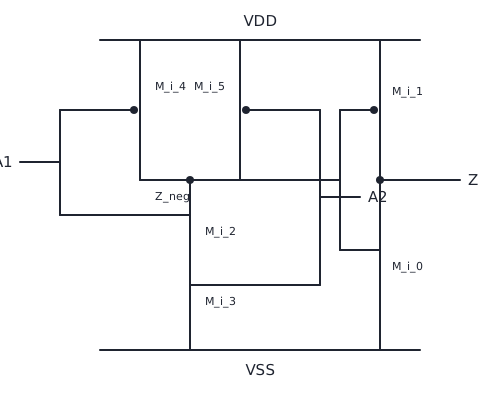
Drawn from PDK netlist `gf180mcu_fd_sc_mcu9t5v0__and2_1.cdl` @ commit `3781fd29` (google/globalfoundries-pdk-libs-gf180mcu_fd_sc_mcu9t5v0), sha256 `c4a48feea59b…436d25`. NAND2 + output inverter, 6 physical devices, 1:1 with this diagram (no folding) — verified device-by-device in issue #1123's PR body.
Renders
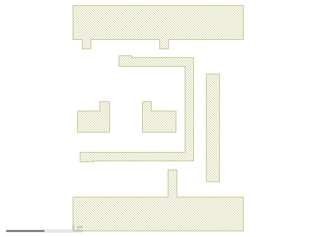
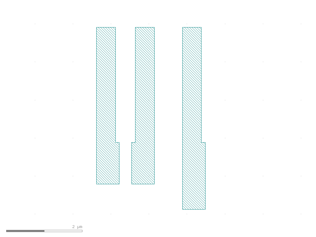
Click a render to open an interactive, pan/zoom viewer of the actual GDS.
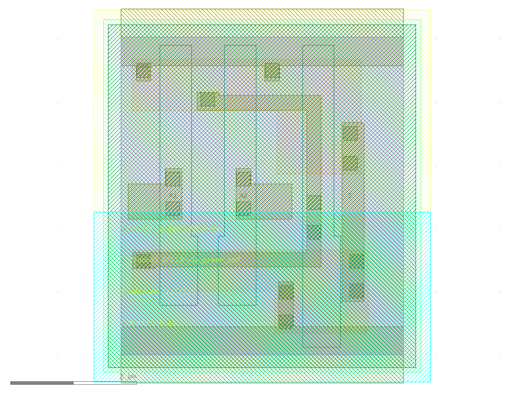 Click to explore →
 Click to explore →
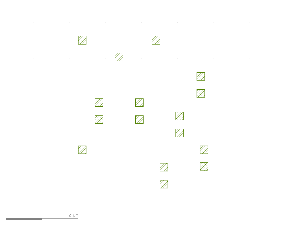 Click to explore →
 Click to explore →
 Click to explore →
 Click to explore →
 Click to explore →
 Click to explore →
 Click to explore →
 Click to explore →
 Click to explore →
 Click to explore →
 Click to explore →
 Click to explore →
Metrics
| Layers | 13 |
|---|---|
| Cells | 1 |
| Instances | 0 |
Signals
Loading waveform…
typical/5.000V/27C
- tphl181.88 ps
- tplh176.15 ps