sky130_fd_sc_hd__inv_1
oksky130 standard-cell layout `sky130_fd_sc_hd__inv_1` from the #4 test corpus.
Schematic
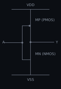
Hand-drawn 2-transistor CMOS inverter topology, illustrating `sky130_fd_sc_hd__inv_1.gds` (sha256 18a9cfa39995…7914c4). See issue #1123 for netlist-derived standard-cell diagrams.
Renders
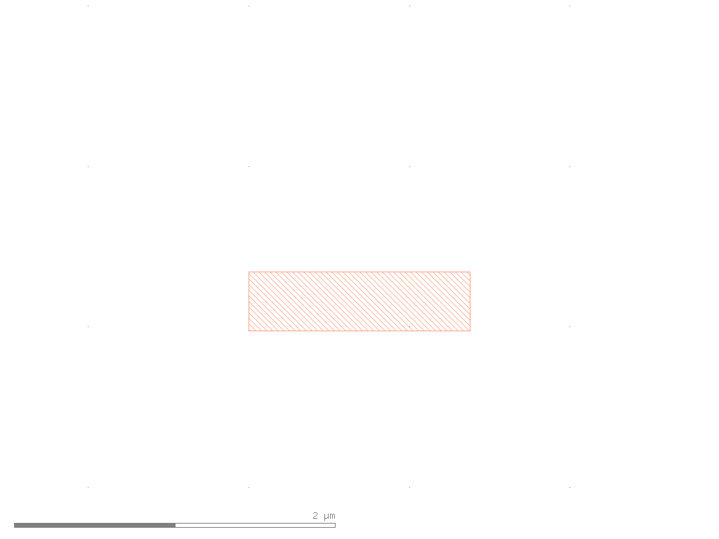
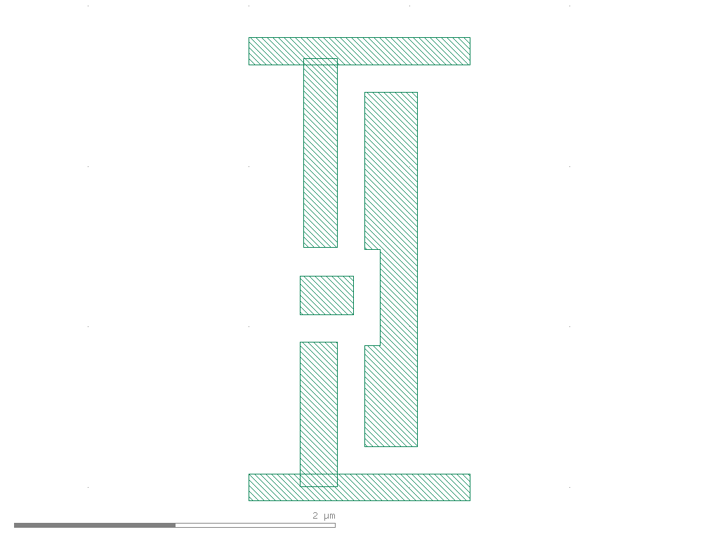
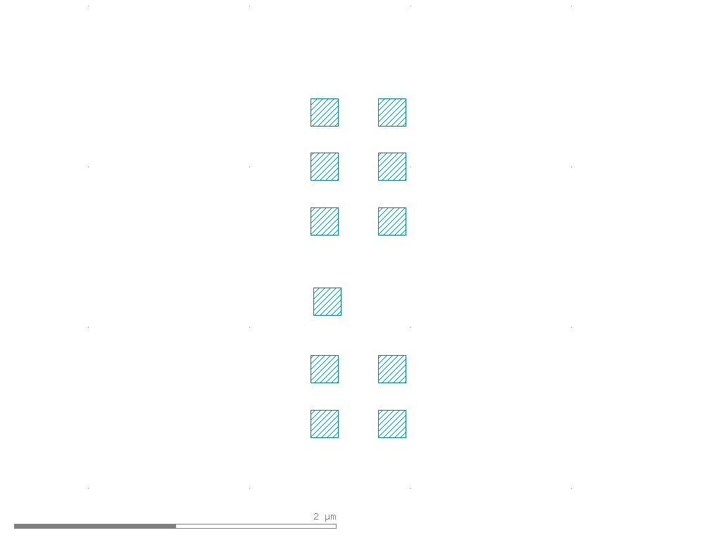
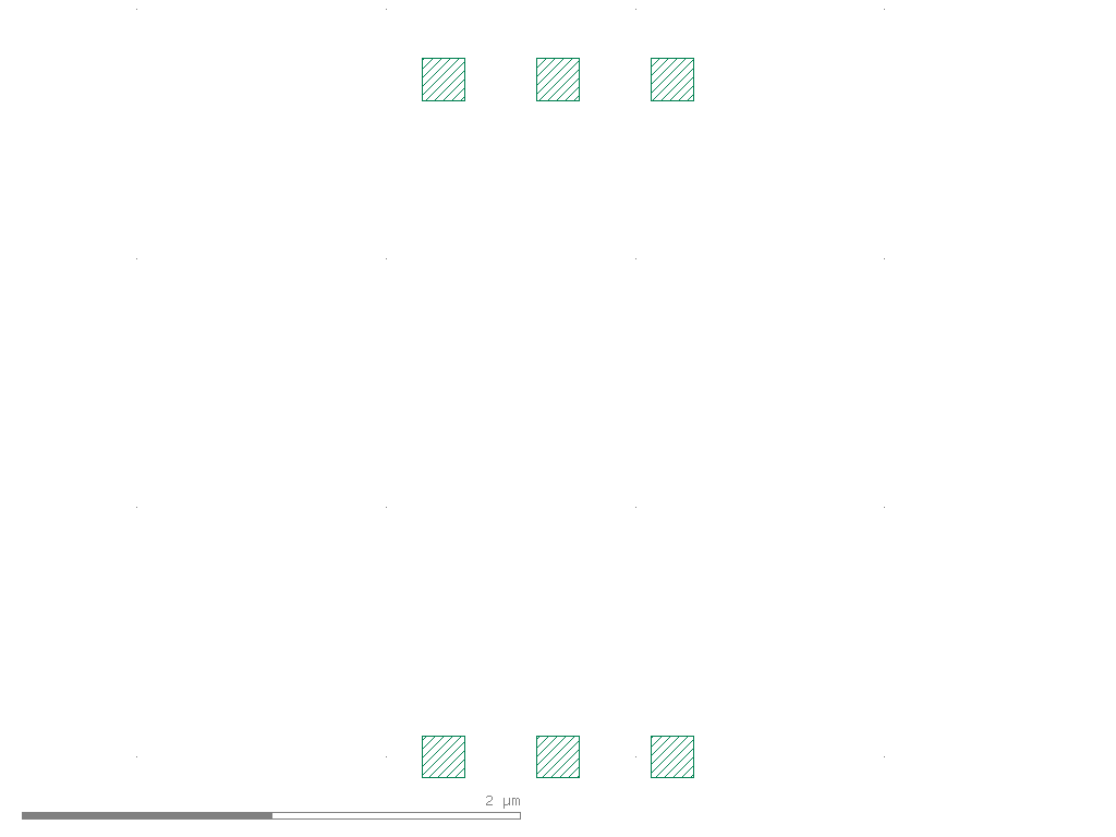
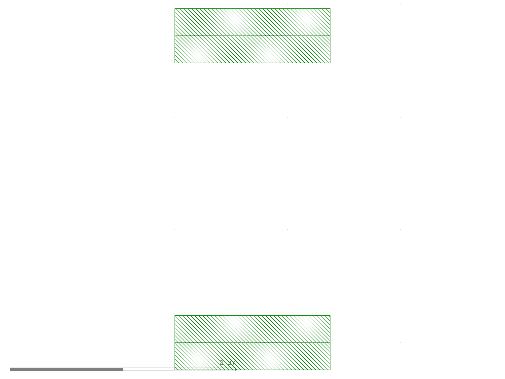
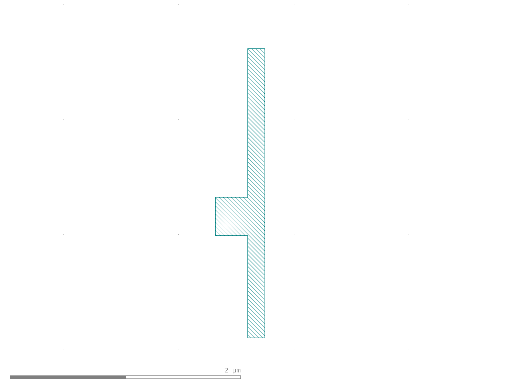
Click a render to open an interactive, pan/zoom viewer of the actual GDS.
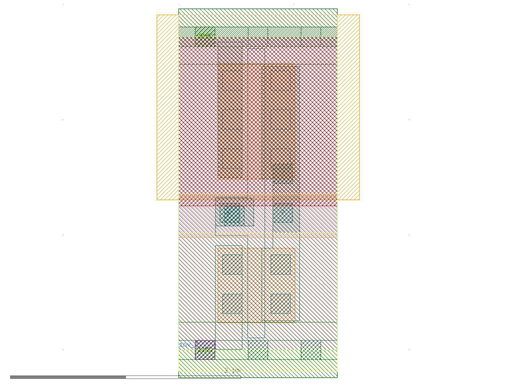 Click to explore →
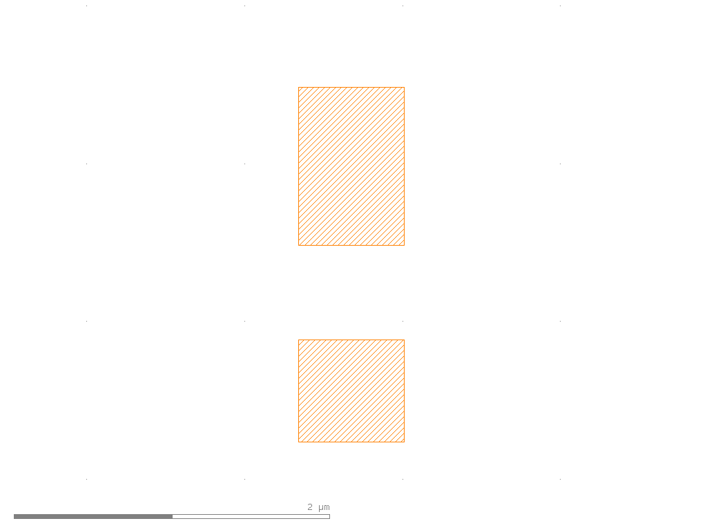 Click to explore →
 Click to explore →
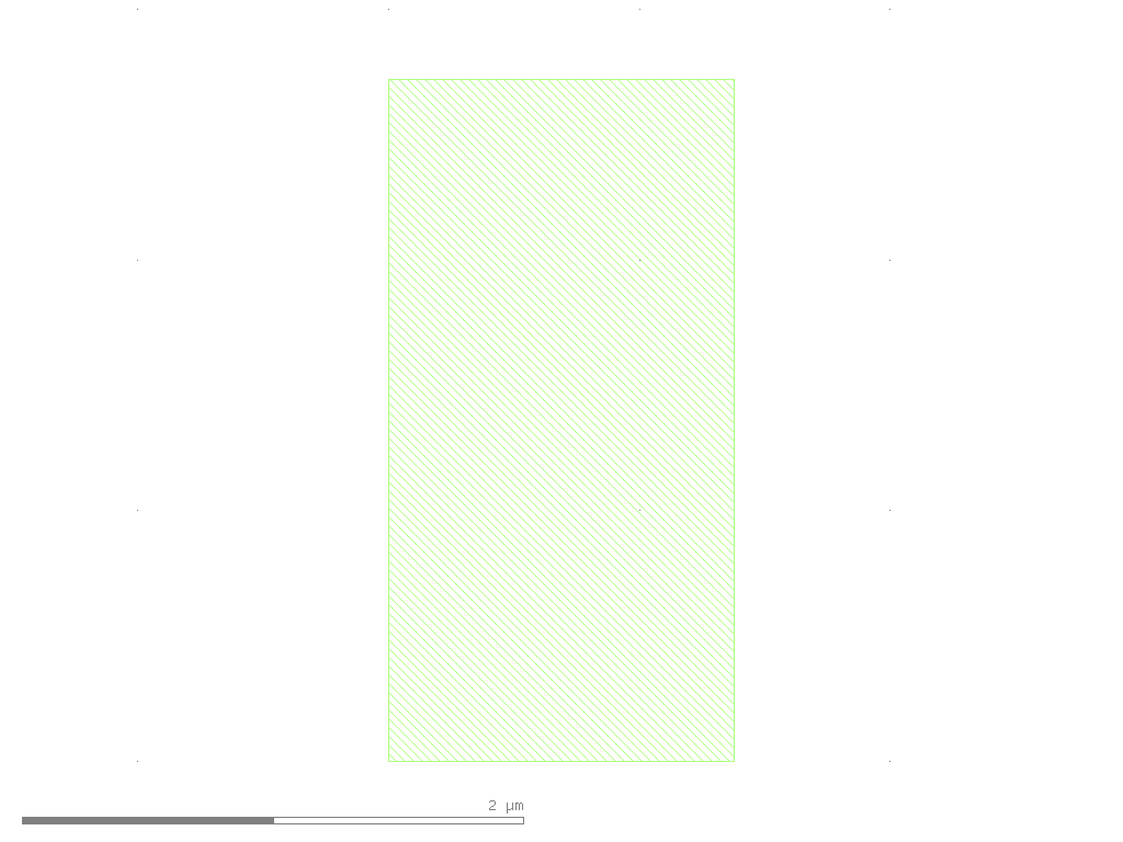 Click to explore →
 Click to explore →
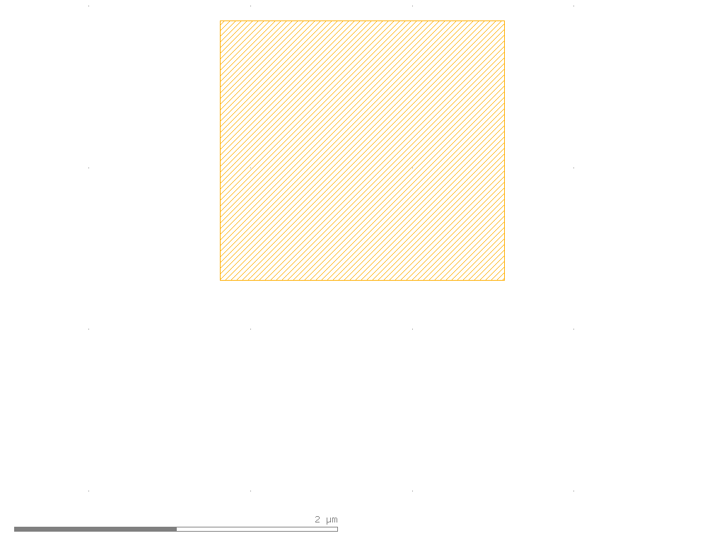 Click to explore →
 Click to explore →
 Click to explore →
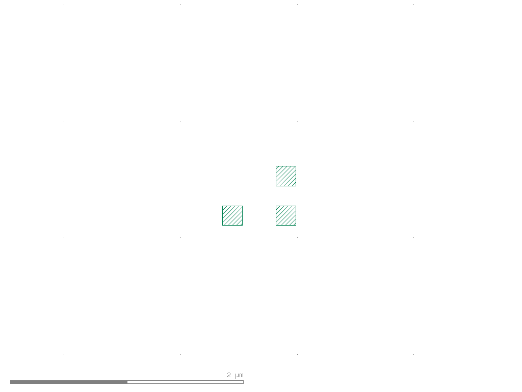 Click to explore →
 Click to explore →
 Click to explore →
 Click to explore →
 Click to explore →
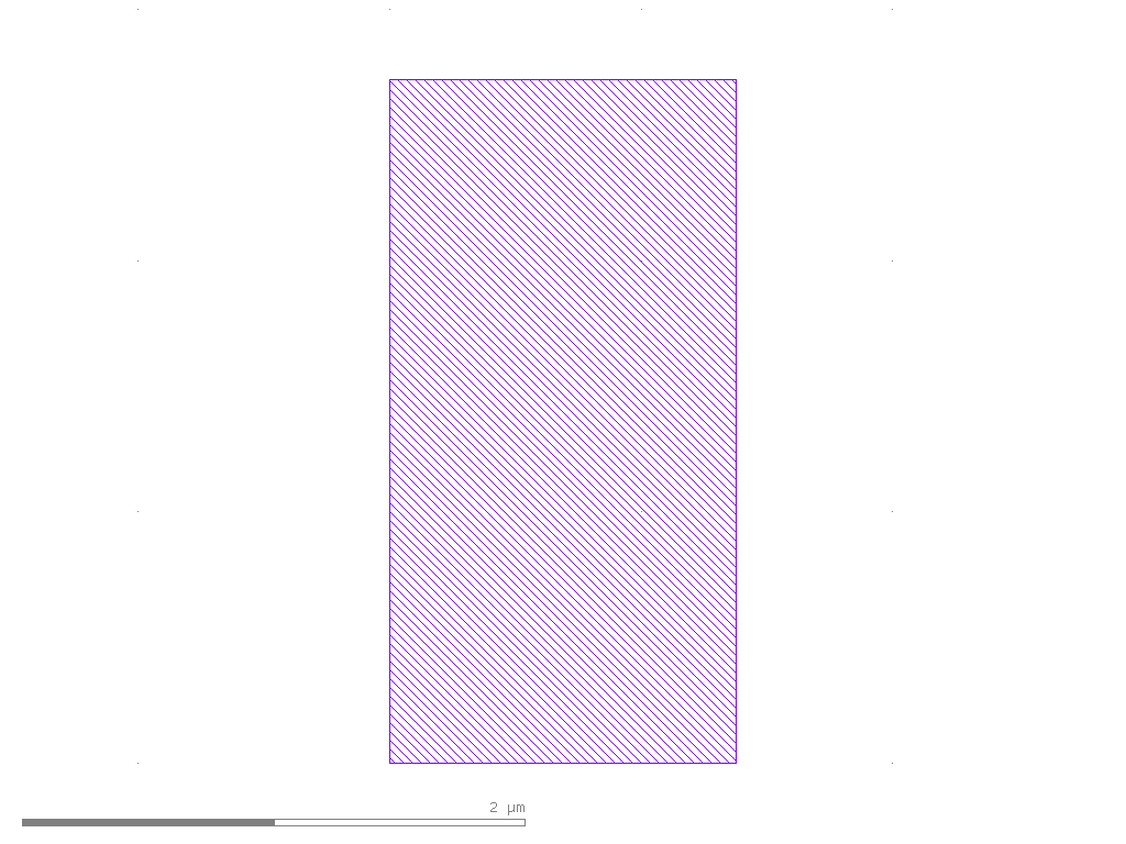 Click to explore →
 Click to explore →
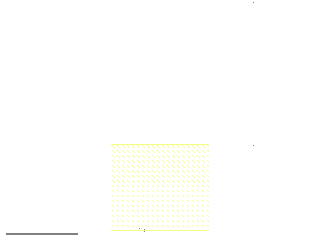 Click to explore →
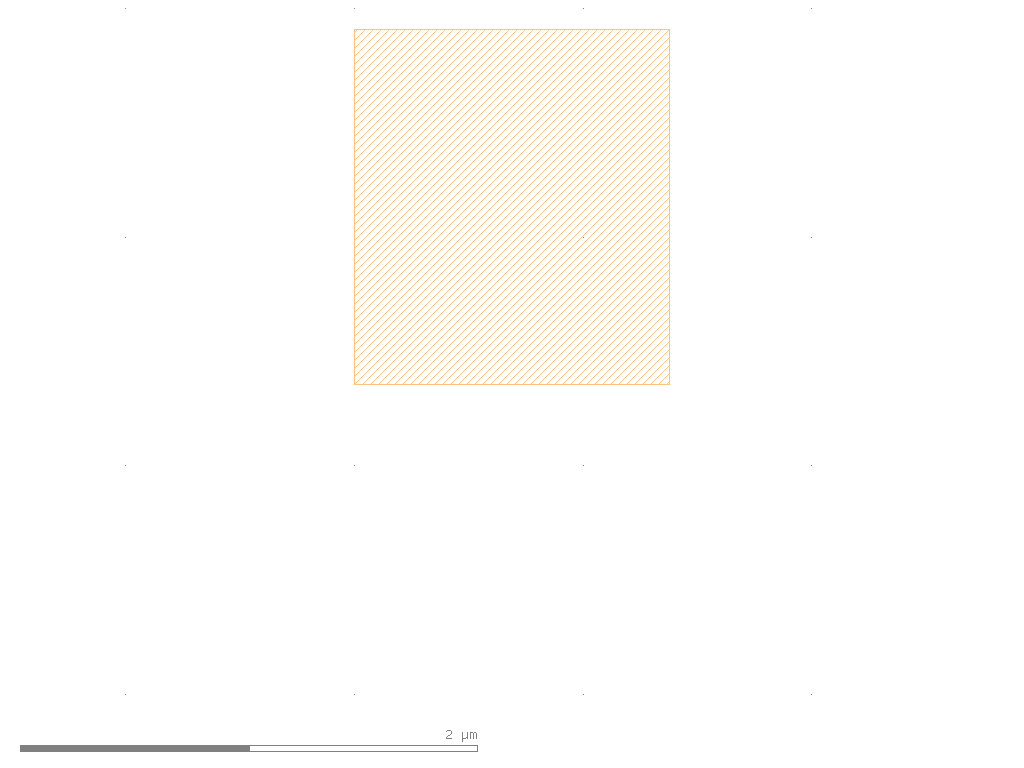 Click to explore →
 Click to explore →
 Click to explore →
 Click to explore →
 Click to explore →
 Click to explore →
 Click to explore →
Metrics
| Layers | 22 |
|---|---|
| Cells | 1 |
| Instances | 0 |
Signals
Edit the stimulus below and re-run to simulate this cell with ngspice in your browser, against the same vendored sky130 device models used to generate the signals above.
Loading waveform…
tt/1.800V/27C
- tphl40.19 ps
- tplh70.12 ps